Gallium Nitride (GaN) Amplifiers in Multiple Carrier Operation
GaN amplifier technology has had a real impact on Block Upconverter and SSPA design for Satcom applications. And it’s a hot buzzword in the industry.
Terrasat have implemented GaN into several IBUC models where it is perceived to deliver benefits for customers. It brings advantages:
- higher power density– delivering higher power in a smaller, lighter enclosure.
- Reduced power consumption.
- Cost reduction in some frequency band–output power combinations.
Terrasat Engineers have implemented techniques to compensate for the inherent nonlinearity of GaN devices. This has resulted in a significant reduction in the amount of output power back-off required to meet the MILSTD definition of Linear Power (PLin) which is the useable output power and standard for comparing BUC/SSPA output power performance.

Graph A
…significant reduction in the amount of output power back-off required to meet the MILSTD definition of Linear Power (PLin)…
Limitations that Deserve Respect
All technologies have their strengths and limitations. It is as important to understand the limitations as it is to know the advantages. With GaN devices, limitations can become evident in operations using more than one carrier. This is not to say that it cannot be used with multiple carriers. But GaN performs differently than GaAs or TWTA amplifiers with respect to multicarrier operation. There are two situations where this limitation should be respected.
First, with a GaAs amplifier, you typically see a relatively linear and continuous IMD3 improvement with output power back-off. Below in Graph A is an IMD3 plot for a 200W C IBUC R GaAs amplifier. (The purple line is the -22 dBc IMD3 part of the MIL-STD linearity definition).

Graph B
GaN performs differently than GaAs or TWTA amplifiers with respect to multicarrier operation.
GaN & GaAs Challenges
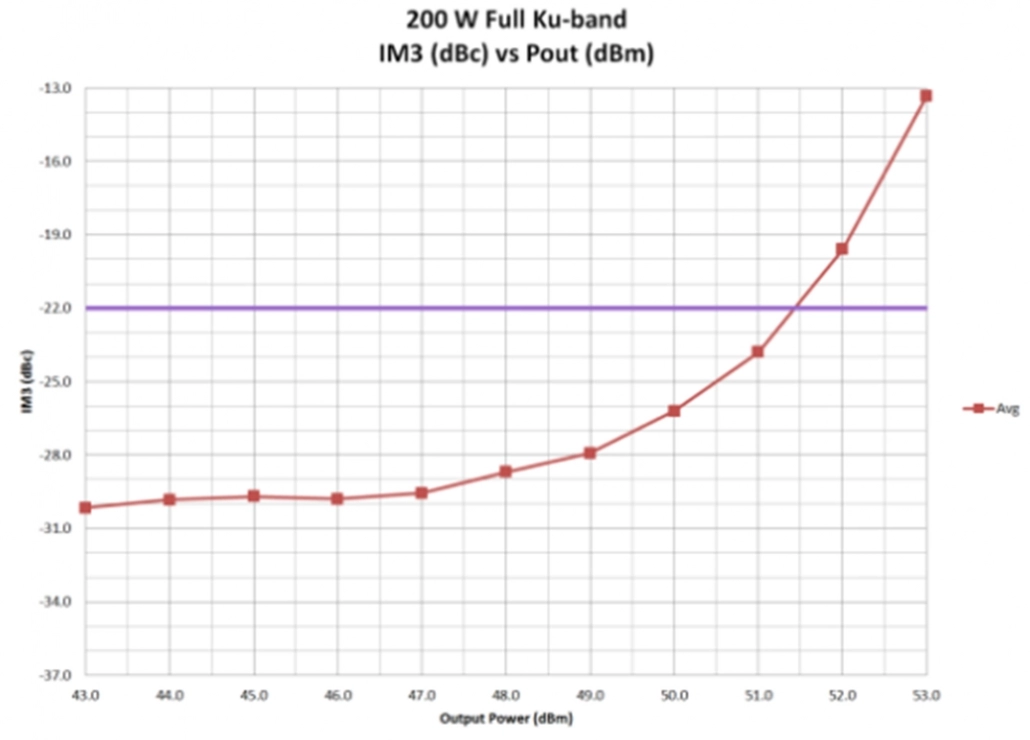
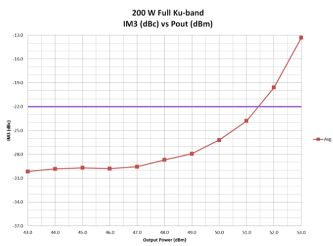
With a GaN unit there is a different result. Please see the IMD3 plot below of a 200W Full Ku IBUC G GaN unit. Things start out fine, but the curve quickly starts to flatten. Then at about 6 dB back-off it hits a “floor”. It doesn’t get any better. This is a characteristic of GaN devices that cannot be overcome.
What this means is that there is a limitation to the quantity of carriers that can be accommodated.
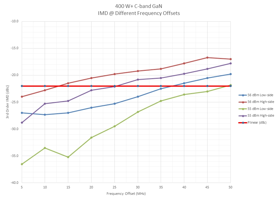
The second limitation is a bit scarier. It only shows up in situations with widely separated carriers. By the MIL-STD definition, all manufacturers measure IMD at a 5 MHz offset for specifications shown on the data sheet. Graph C shows IMD products at wider offsets.
The red line is the defined -22 dBc IMD level. The other lines plot IMD above and below the test channels at saturated power and then with 1 dB of output power back-off. At the 5 MHz offset there is clearly no problem meeting the -22 dBc requirement. However, this shows how the intermodulation products are increasing in intensity as the carrier offset increases. Whereas logic from working with amplifiers would say that the further two carriers are from each other, the less they will interact, it turns out that the opposite is true with GaN devices. With carriers spaced more than 25 MHz apart, there will be intermodulation products that may interfere with other services.

Graph C


